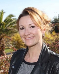
Catherine Alix‐Panabières
Liquid biopsy in cancer: Technical challenges and clinical applications
The development of blood-based, tumor-specific biomarkers called real-time liquid biopsy such as circulating tumor cells (CTCs) have made significant advances over the last years in cancer research.
Highly-sensitive liquid biopsy assays have been developed and are applied to detect minimal residual disease, to get prognostic information and to monitor therapy efficiency.
In my talk, I will present the new EPIDROP technology that detect viable CTCs. It allows the enumeration/characterization of all CTCs, and gives information on their functionality at the single cell level and also on their drug resistance profile in a few hours: developing an oncogram for the real-time follow-up of resistance against chemotherapy or immunotherapy is urgently needed.
Biography
Dr Catherine Alix-Panabières received her PhD-degree in Strasbourg (1998). She is associate professor - director of the Laboratory of Rare Human Circulating Cells at the UMC Montpellier. These last 20 years, she put huge efforts on the analysis of circulating tumor cells in cancer patients. She coined for the first time ‘Liquid Biopsy’ in 2010 (Trends Mol Med) with Klaus Pantel. She authored >110 scientific publications and is the inventor of 3 patents in the liquid biopsy field. She received the Gallet et Breton Cancer Prize (2012) and the 2017-AACR-Award for the most cited article in 2015 (Cayrefourcq. Cancer Res).
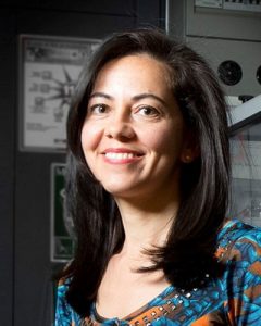
Hatice Altug
Frontiers in Nanophotonics: Enabling Technology for Next-Generation Biosensors
Nanophotonics, which excels at generating enhanced light-matter interactions and sub-wavelength light confinement, enables light manipulation in new ways. We exploits nanophotonics to introduce powerful bioanalytical tools that can have impact on areas including life science research, diagnostics and safety. We exploit nanoplasmonics and all-dielectric metasurfaces to develop nanophotonic biochips and investigate nanofabrication methods for their low-cost manufacturing. We integrate photonic biochips with microfluidics for sample handling. We use data science tools with hyperspectral and bioimaging to achieve high device performance. In this talk, I will present some of our recent work and provide their prospects in biomedical and clinical applications.
Biography
Hatice Altug is full professor at Ecole Polytechnique Federale de Lausanne and the director of Doctoral School in Photonics. She received her Ph.D. in Applied Physics from Stanford University. Prof. Altug is the recipient of the U.S. Presidential Early Career Award for Scientists and Engineers, OSA Adolph Lomb Medal, EPS Emmy Noether Distinction, elected fellow of the OSA, IEEE Photonics Society Young Investigator Award. She received prestigious grants including ERC Consolidator and Proof-of-Concept Grants, U.S. ONR Young Investigator Award, U.S. NSF CAREER Award. She won Inventors’ Challenge competition of Silicon Valley and named to Popular Science Magazine’s "Brilliant 10" list.
Athanassia Athanassiou
Development and Engineering of Biocomposites for applications in Wound Management and Water Treatment
Unique properties of natural polymers such as controlled biodegradability, biocompatibility, low toxicity, low costs make them ideal candidates to substitute conventional polymers. When they are manufactured into specific geometries, the developed systems become very efficient in biomedical applications and water remediation. Regarding biomedical applications multi-layered films, fibrous membranes, emulsions, microparticles, and coatings will be presented with unique capabilities in wound management and other biomedical areas. Regarding water treatment, it will be reported the manufacturing of structures with well-controlled porous or fibrous configurations, based on natural polymers and molecules, modified for optimized interactions with selected components of the water under treatment.
Biography
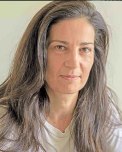
Athanassia Athanassiou is Principal Investigator at the Istituto Italiano di Tecnologia (IIT, Genoa, Italy). She has a degree in Physics from the University of Ioannina in Greece, an MSc from the University of Manchester and a Ph.D. in Physics from Salford University in UK. From 2000 to 2005, she worked at FORTH in Crete, and in 2006 she became Senior Researcher at NNL, CNR-Istituto di Nanoscienze, Lecce. In 2011, she joint IIT and nowadays her group of Smart Materials counts 50 people that work on sustainable materials and technologies for the benefit of environmental and human health. She has published more than 350 articles in scientific journals and 22 patents.
Fabio Biscarini
Nanoscale effects in organic transistors for bio- and neuroelectronics via thin film growth, interfacial chemistry and patterning
I will discuss three organic transistor architectures used as biosensors, transducers of bioelectric signals, and neuromorphic devices. I will show the combined use of thin film growth by high vacuum sublimation, solvent- assisted and patterning techniques in organic device fabrication. I will highlight the importance of technological control of the nanoscale morphology and chemistry in such devices, showing the large effects that apparent subtleties yield in the response, sensitivity, selectivity and operational conditions of such devices, especially in the context of diagnostics and in vivo applications.
Biography
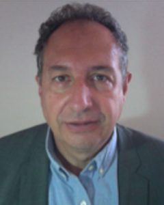
Fabio Biscarini is Professor of Chemistry at University of Modena and Reggio Emilia (2013-) and Principal Investigator at IIT, heading the “Organic Neuroelectronics” research line in Ferrara (2017-). He received laurea in Industrial Chemistry cum Laude-Università di Bologna (1986), Ph.D. in Chemistry-University of Oregon (USA) (1993). He was CNR Bologna as postdoc (1994-1995), Researcher (1996-2001), Senior Scientist (2002-2010), Research Director (2010-2013). He authored >270 publications with >12000 citations and h-index 63 (Google Scholar), coordinated EU (10) and National (4) projects, co-invented 20 patents, and founded Scriba Nanotecnologie (2005-2021), Nano4bio (2008-2015), Organic Bioelectronics (2019-). He was awarded 2012 Premio Sapio Industria, 2007 EU-Descartes Prize, and is Member of Academia Europaea (2021-), Fellow of the Royal Society of Chemistry (2004-), and Member of Accademia delle Scienze di Modena (2017-).
Rosa Cordoba
Direct-writing of advanced nano-superconductors and devices using Focused Ion Beams
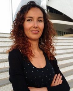
Superconductors are dissipationless carriers of electric current and provide macroscopic, and thus robust, quantum coherence. To achieve the required performance employed in applications as magnetic sensors, nowadays bulk superconductors frequently need nanoscale engineering. Interestingly, when these materials are reduced to the nanoscale becoming nano-superconductors, novel exciting physical phenomena emerge. This has encouraged the study of their performance in the three dimensions as key elements that would be implemented into superconducting circuits. Nevertheless, the fabrication and characterization of nano-superconductors in the three dimensions are still challenging. Here, I introduce a direct-write nanolithography method based on focused ion beam technologies to fabricate at-will advanced nano-superconductors. Particularly, I have prepared superconducting W-C nanostructures in the three dimensions by decomposing tungsten hexacarbonyl molecules with a highly-focused He+ or Ga+ ion beam.
Biography
Dr. Córdoba is a world expert in the preparation and characterization of advanced nanomaterials created in the three dimensions, particularly in superconducting and magnetic nanostructures.
Since 2019, Junior Leader fellow, Institute of Molecular Science (ICMol), University of Valencia, Spain. Young Investigator Award and Lecturership 2020 by Elsevier, MEE journal. To honour and promote a Young researcher in Nanofabrication and Nanotechnology for Physics.
Scientific co-coordinator 2D Materials research line, U. Excellence María de Maeztu, ICMol (2020-2023). PhD in Physics (2012), Condensed Matter Physics Department, University of Zaragoza, Spain. 58 scientific publications in HI peer-reviewed international journals (Nature Phys., Nature Comm., Nano Letters, ACS Nano, Phys. Rev. Lett., Adv. Elec. Mat., Nature Sci. Rep.), 1 book and 5 book chapters. h-index: 22; Citations: 1372.

Yasin Ekinci
Advancing the photolithography for more Moore
The steady shrinkage of the semiconductor devices in the last five decades, as predicted by Moore’s law, has changed our daily lives. This progress was possible through advancements in photolithography. Extreme ultraviolet (EUV) lithography at 13.5 nm wavelength is the manufacturing method for high-volume semiconductor manufacturing at 7 nm technology node and below. To enable future progress, many challenges lie ahead. In addition to the optical resolution, other limitations are already emerging, such as photon shot noise, mask 3D effects, and, not the least, resist materials. In this presentation, some of these issues will be addressed, and potential solutions are proposed.
Biography
Yasin Ekinci is the head of the Laboratory for Micro and Nanotechnology (LMN). He obtained his Ph.D. in Max-Planck Institute for Dynamics and Self-Organization, Göttingen, Germany, in 2003. He worked on various topics of nanoscience and technology, including atom optics, surface science, EUV lithography, resist materials, coherent scattering, lensless imaging, plasmonics, metamaterials, biosensing, semiconductor nanostructures, and nanofluidics. He is author/co-author of more than 200 papers, 3 book chapters, and 7 patent applications. He received Young investigator of the year award of Swiss Society for Optics and Microscopy in 2009. He is a fellow of SPIE.

Georg Fantner
Institute of Bioengineering, EPFL, Lausanne, 1015, Switzerland
Recent Developments in Cantilever Technology for High-Speed AFM
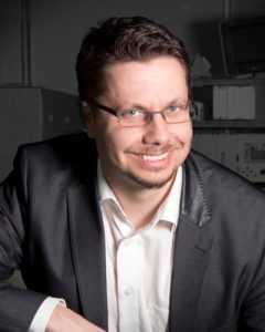
The invention of microfabricated cantilevers by Quate et al. was essential for the success of atomic force microscopy (AFM). Innovation in AFM technology still goes hand in hand with the development of new cantilever technology. This is particularly true for the field of high-speed AFM, where small cantilevers were essential for improving the imaging speed. In our work we explore new approaches to improve the speed and usability of AFM through the development of custom cantilevers.
Biography
GEORG E. FANTNER received his PhD degree from UC Santa Barbara in 2006. After a Postdoc in the biomolecular materials lab at the Massachusetts Institute of Technology, he joined the École Polytechnique Fédéral de Lausanne as assistant professor in 2010. Now, as associate professor, he leads the laboratory for bio- and nano-instrumentation in the institute for bioengineering. His research focusses on the development of new technologies to measure and manipulate nanoscale structures in general, and the development of atomic force microscopy instrumentation in particular. His recent work focusses on new modes for high-speed AFM imaging of molecular processes, as well as long-term time lapse imaging of cellular processes. Prof. Fantner hold several patents in the field of nanotechnology and is the co-founder of two nanotechnology companies.
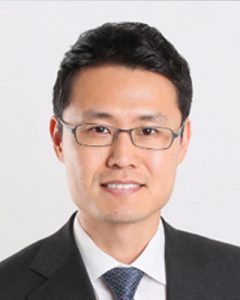
Jae-Woong Jeong
Design Strategy for Mechanically Transformative Electronics, Sensors, and Implantable Devices
Conventionally, electronics are constructed with static form factors to serve targeted applications. For examples, emerging soft wearable electronics are designed to allow dynamic accommodation of applied stress to maximize user comfort when integrated with the body. In contrast, rigid electronics are built for tabletop or handheld uses based on their solid interfaces that ease user handling. To leverage advantages of both rigid and soft electronics, we developed a new class of electronics that can reconfigure their shape, flexibility and stretchability for desired purposes. This talk will introduce the concept, materials, and operation principle of transformative electronics with applications in wearables, implantables, and sensors.
Biography
Dr. Jae-Woong Jeong is an Associate Professor of Electrical Engineering at Korea Advanced Institute of Science and Technology (KAIST). He received his PhD degree in electrical engineering from Stanford University in 2012, and worked as a postdoctoral research associate at the University of Illinois at Urbana-Champaign from 2012 to 2014. Before joining KAIST, he was an Assistant Professor of Electrical, Computer & Energy Engineering at University of Colorado, Boulder from 2015 to 2017. Dr. Jeong’s research focus is in soft bio-integrated electronics and systems for advanced healthcare and brain research.
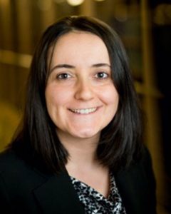
Duygu Kuzum
Transparent Neural Interfaces for Multimodal Probing Brain Circuits
Understanding neuronal dynamics and information processing performed by neural circuits requires advanced technologies with high-resolution sensing and stimulation capability. Optically transparent neural interfaces can enable integration of optical imaging, optogenetics and electrophysiology. In this talk, I will present our recent work on graphene-based transparent neural interfaces, highlight key applications and discuss processing multimodal datasets.
Biography
Duygu Kuzum received her Ph.D in Electrical Engineering from Stanford University in 2010. She is currently an Associate Professor in Electrical and Computer Engineering Department at University of California, San Diego. Her research focuses on applying innovations in nanoelectronics to develop new technologies, which will help to better understand circuit-level computation in the brain. She was a recipient of a number of awards, including Innovators under 35 (TR35) by MIT Technology Review (2014), ONR Young Investigator Award (2016), IEEE Nanotechnology Council Young Investigator Award (2017), NSF Career Award (2018), NIH NIBIB Trailblazer Award (2018), and NIH New Innovator Award (2020).

Thomas Laurell
Acoustic isolation of extracellular vesicles - From uL/min to mL/min
Isolation of nanobioparticles from suspension commonly requires extended ultracentrifugation and manual handling protocols. Microfluidics in combination with acoustics have in more recent years opened new avenues to nanoparticle manipulation. Acoustic seed trapping is a technology that utilizes inter particle forces derived from sound scattered at particles in suspension and enables submicron particle enrichment. In biomedicine extra cellular vesicles (EV) (i.e. submicrometer vesicles, shed from cells) gain a lot of attention as potential carriers of biomarkers. We have previously pioneered the development of acoustic seed trapping of EVs in biofluids (≈10-100 uL samples) for biomarker analysis. In order to broaden the applicability of acoustic seed trapping, processing of larger sample volumes are needed. We now show the upscaling of acoustic EV isolation in urine from the 10-100 uL/min to mL/min range and demonstrate a 40X capacity increase of seed particles. The capacity increase enabled rapid isolation of urine EVs for subsequent mapping of differential proteome profiles of urine vs. the urine EV fraction as monitored by mass spectrometry. The current EV isolation platform now provides a rapid route to defined EV-based sub proteomes in biofluids.
Biography
Thomas Laurell is a professor since 2000 at the Dept. Biomedical Engineering at Lund University, Sweden. His research focus is microtechnology and microfluidics in life sciences. He has pioneered chip integrated acoustofluidics which currently also is his main focus. He is a co-founder of the Chemical and Biological Microsystems Society (CBMS) and served as President for CBMS 2010- 2017. Laurell is a co-founder of AcouSort AB and is an elected member of: The Royal Swedish Academy of Sciences; The Royal Swedish Academy of Engineering Sciences and a Fellow of School of Engineering, The University of Tokyo. Since 2019 he is a Swedish Research Council Distinguished Professor and an Honorary visiting professor at University Putra Malaysia.

Liam O’Faolain
Tyndall National Institute, Cork - Ireland
Silicon based Metalenses for tight focusing of light
Metasurfaces are ultrathin-film optical elements that can manipulate the amplitude, phase, and polarization of light. The need to minaturise optical elements has generated a significant research effort on the realisation of flat structures to focus light such as subwavelength gratings and metamaterials. To date, most of these structures manipulate a linearly polarised incident beam, whereas the use of radially or azimuthally polarised light offers important advantages. In this work, we use metasurfaces to simultaneously convert linearly polarized incident light into an azimuthally polarized optical vortex and focuses the at a distance approximately equal to the wavelength of the incident light.
Biography
Liam O’Faolain leads the Nanophotonics Group at the Centre for Advanced Photonics and Process Analysis. His research group focuses on developing efficient lasers and innovative sensors based on nanophotonics and integrated photonics, see www.cappa.ie . He is the author/co-author of more than 100 journal papers. His ”h"-factor is 48. He is currently supervising 13 PhD students and 5 postdoctoral research fellows. He co-ordinates the ERC Proof of Concept project HERCULES, the OPTHAPHI Marie Curie European Joint Doctorate project (https://www.optaphi.eu/) and the H2020 PASSEPARTOUT project (https://www.passepartout-h2020.eu/).
Eitan Oksenberg
Energy-selective plasmonic nanoreactors
Plasmonic resonances can concentrate light into exceptionally small volumes, approaching the molecular scale. The extreme light confinement provides an advantageous pathway to probe molecules at the surface of plasmonic nanostructures with highly sensitive spectroscopies, such as surface-enhanced Raman scattering. Unavoidable energy losses associated with metals, which are usually seen as a nuisance, carry invaluable information on energy transfer to the adsorbed molecules through the resonance linewidth. We measured a thousand single nanocavities with sharp gap plasmon resonances that spanned the red to near-infrared spectral range and used changes in their linewidth, peak energy and surface-enhanced Raman scattering spectra to monitor the energy transfer and plasmon-driven chemical reactions at their surface. Using methylene blue as a model system, we measured shifts in the absorption spectrum of molecules on surface adsorption and revealed a rich plasmon-driven reactivity landscape that consists of distinct reaction pathways that occur in separate resonance energy windows.
Biography
Dr. Eitan Oksenberg obtained his PhD from the Weizmann Institute of Science for which he received two awards for outstanding PhD research. In his research at the Department of Materials and Interfaces, he investigated the surface-induced growth and properties of nanowires of optoelectronic materials, exploring both classic and soft semiconductors and integrating them into various optoelectronic devices including patented photovoltaic devices. In 2018 he moved to Amsterdam and joined the Center for Nanophotonics and the Light Management in New Photovoltaic Materials team at AMOLF as a post-doctoral researcher. His research lies at the interface of chemistry and nanophotonics dedicated to find new ways to harness amplified light-matter interactions to control chemical reactions.
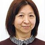
Haiyan Ou
Nano-engineering unlocks the potential of SiC for photonics
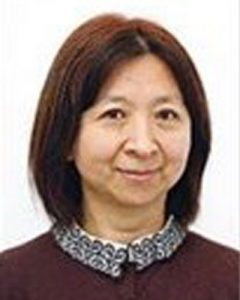
Silicon carbide (SiC) has already been used widely for abrasives, light-emitting diodes and transistors. Recent nanotechnology advances have enabled it an emerging scalable material platform for integrated nonlinear and quantum photonics, outperforming its counterparts such as diamond, III-V semiconductors and Si etc. in some aspects. This talk will present the key nanotechnologies to make high-performance nanophotonic devices based on SiC on insulator (SiCOI) platform and review the state of the art of SiCOI based nonlinear and quantum devices. At last, the prospect and challenges of SiCOI platform will be discussed for fully unlocking its potential in photonics.
Biography
Haiyan Ou, PhD in 2000 from Institute of Semiconductors of Chinese Academy of Sciences, associate professor since 2005 at Technical University of Denmark (DTU). Her research interest is primarily in semiconductors materials and devices for integrated optics, photovoltaics and light emission. She has been working on integrated optics for 23 years being especially involved in several research activities and projects on building blocks for integrated optics, silica-on-silicon arrayed waveguide gratings, nonlinear integrated waveguides, silicon photonics for optical communications, innovative solution for next generation communication infrastructure etc. She is a PI/WP leader in LEDSiC (a new type of white light-emitting diode using fluorescent silicon carbide), NORLED (Nordic light-emitting diode initiative). She is coordinating an EU horizon 2020 FET Open project SiComb (CMOS compatible and ultrabroad-band on-chip SiC frequency comb).
Junsuk Rho
Dynamic metaphotonics for structural colors and holographic displays
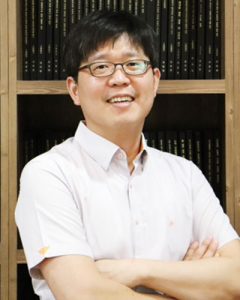
Flat optics, which is realized by the artificially created two-dimensional material platform called optical metasurfaces, is currently undergoing a science-to-technology transition. A representative example includes a flat and ultra-compact metalens, which has huge potential for replacing conventional bulky and heavy optical lens. However, ‘real-time’ active operations of those flat optical devices have remained unresolved yet. To resolve such a grand challenge, we propose two approaches to realize dynamic metaphotonic devices using multiple light properties and tunable materials. We believe such dynamic metaphotonic devices will further accelerate real-life applications such as video holographic-displays, full-color high resolution displays, focus-tunable metalenses and LiDARs.
Biography
Dr. Junsuk Rho received his B.S. degree from Seoul National University in 2007, M.S. degree from the University of Illinois Urbana-Champaign in 2008, and Ph.D. degree from the University of California, Berkeley in 2013. He was the Ugo Fano fellow in Nanoscience and Technology Division at Argonne National Laboratory, USA. Since 2014, he has been an Assistant Professor, Associate Professor, Mu-Eun-Jae Endowed Chair Professor and Young Distinguished Professor at Pohang University of Science and Technology (POSTECH), Korea. His research includes metamaterials, plasmonics, nanophotonics and nanofabrication. Dr. Rho is a recipient of the Korean Presidential Early Career Award in 2019 and MEE/MNE Young Investigator Award and Lectureship in 2020. He currently serves as Associate Editors of Light: Science and Applications (Springer-Nature) and Micro and Nano Engineering (Elsevier).

Elisa Riedo
New York University, New York – USA
Reusable Millimeter Size Bone Tissue Replicas With Sub-15 nm Feature Size on A Biocompatible Polymer

The ability to replicate the microenvironment of biological tissues creates unique biomedical possibilities for stem cell applications. Current fabrication methods are limited by either the control on feature size and shape, or by the throughput and size of the replicas. Here, a novel platform is reported that combines thermal scanning probe lithography (tSPL) with innovative methodologies for the low-cost and high-throughput nanofabrication of large area quasi-3D bone tissue replicas with high fidelity, sub-15 nm lateral precision, and sub-2 nm vertical resolution [1]. This bio-tSPL platform features a biocompatible polymer resist that withstands multiple cell culture cycles, allowing the reuse of the replicas, further decreasing costs and fabrication times. The as-fabricated replicas support the culture and proliferation of human induced mesenchymal stem cells, which display broad therapeutic and biomedical potential. Furthermore, it is demonstrated that bio-tSPL can be used to nanopattern the bone tissue replicas with amine groups, for subsequent tissue-mimetic biofunctionalization. The achieved level of time and cost-effectiveness, as well as the cell compatibility of the replicas, make bio-tSPL a promising platform for the production of tissue-mimetic replicas to study stem cell-tissue microenvironment interactions, test drugs, and ultimately harness the regenerative capacity of stem cells and tissues for biomedical applications.
[1] “Cost and Time Effective Lithography of Reusable Millimeter Size Bone Tissue Replicas With Sub-15 nm Feature Size on A Biocompatible Polymer” Advanced Functional Materials, (2021) https://doi.org/10.1002/adfm.202008662
Biography
Professor Elisa Riedo received her Ph.D. in Physics in a joint program between the University of Milano and the European Synchrotron Radiation Facility in Grenoble, France. In 2003 she was hired as Assistant Professor at the Georgia Institute of Technology in the School of Physics, where she was promoted to full Professor in 2015. Since 2018, she is a Professor at the NYU Tandon School of Engineering in the department of Chemical and Biomolecular Engineering, where she is also Chief Inclusivity Officer. Her research is focused on new scanning probe microscopy- based methods to study and fabricate materials and solid/liquid interfaces at the nanoscale. Highlights from her research are the invention of thermochemical nanolithography, the discovery of the exotic viscoelasticity of nano-confined water, and the first observation of the exceptional mechanical properties of diamene, pressure induced single layer diamond. In 2013, Dr. Riedo was elected APS Fellow, in the Division of Condensed Matter Physics.

Pino Strangi
CNR Nanotec & University of Calabria - Italy
Hyperbolic Dispersion Metasurfaces and Fano Resonance Optical Coatings for Chiroselective Biosensing
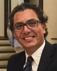
In recent years a wide interest has been spurred by the inverse design of artificial layered heterostructures for nano-biophotonic applications. In particular, the extreme optical properties of artificial hyperbolic dispersion nanomaterials allowed access to new physical effects and mechanisms. The unbound iso-frequency surfaces of hyperbolic metamaterials and metasurfaces sustain virtually infinite photonic density of states, ultrahigh confinement of electromagnetic fields and anomalous wave propagation. Here, we present the physics of different deeply subwavelength layered heterostructures and how they allow light-matterinteraction at the single nanometer scale, including within living systems.
Biography
Giuseppe Strangi(http://physics.case.edu/faculty/giuseppe-strangi/) is Professor of Physics and Ohio Research Scholar in Surfaces of Advanced Materials at Case Western Reserve University. He leads the Nanoplasm Labs (http://nanoplasm.case.edu) at CWRU Cleveland, and he is research director of the National Research Council (CNR- Italy). Strangi is the President of the Scientific Committee of the Foundation “Con il Cuore”, a national foundation that supports cancer research in Europe and he is the General Chair of the International Conference – NANOPLASM “New Frontiers in Plasmonics and Nanophotonics”. Strangi research interests include condensed matter physics, nano-photonics and plasmonics of electromagnetic materials and cancer nanotechnology. He is fellow of The Institute of Science of the Origins, Case Comprehensive Cancer Center (CWRU) and Fellow of The Optical Society of America (OSA).
Toshiyuki Tsuchiya
Wineglass mode MEMS gyroscopes with single crystal materials
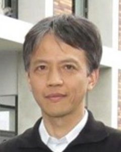
Two types of wineglass mode MEMS gyroscope with single crystal materials have been developed for achieving high performance to be utilized for inertial navigation system. One is (100) silicon ring resonator gyroscope with geometrical compensation. The modified ring width according to its anisotropic elasticity reduces the electrostatic tuning voltage and angle random walk in operation. The other is piezoelectric disk gyroscope with lithium niobate. Because of its high electromechanical coupling coefficient and high quality factor, higher performance is expected. We have demonstrated gyroscope operation using 155°-Y-cut wafer for mode matching of two wineglass modes.
Biography
Toshiyuki Tsuchiya received his M.S. degree from the University of Tokyo, Japan, and his Ph.D. degrees from Nagoya University, Japan, in 1993, and 2002, respectively. He worked with Toyota Central Research and Development Laboratories from 1993 to 2004. Then, he joined Kyoto University as an associate professor and since 2019 he is a professor in the Department of Micro Engineering, Kyoto University, Japan. He is currently engaged in the research of MEMS fabrication, inertial sensors, and the reliability of micro/nano material and devices.
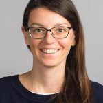
Silvia Vignolini
Biomimetic colour engineering: from nature to application
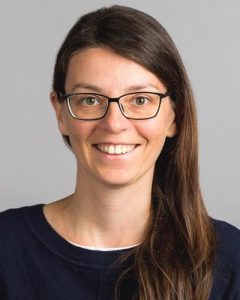
The most brilliant colours, photonic colouration in nature are obtained by nano-structuring transparent materials. In this seminar, I will introduce some striking examples of natural photonic nanostructures and share some insight on their development. Then I will review our recent advances to fabricate bio-mimetic photonic nano structures using only biopolymers.
Biography
Prof Silvia Vignolini studied Physics at the University of Florence, Italy. In 2009, she was awarded a PhD in Solid State Physics at the European Laboratory for non-Linear Spectroscopy and the Physics Department at the University of Florence. In 2010, she moved to Cambridge as a post-doctoral research associate working in the Cavendish Laboratory and the Plant Science Department. In 2013, she started her independent research becoming a BBSRC David Philip Fellow. Dr. Vignolini is currently a Professor at the University of Cambridge in Sustainability and Bio-inspired materials. Her research interest lies at the interface of chemistry, soft-matter physics, optics, and biology. In particular, her research focuses on the study of how natural materials (like cellulose) are assembled into complex architectures within living organisms and how the such materials can be exploited to fabricate a novel class of photonic pigments.

Martin Wegener
3D Laser Nanoprinting: Recent Progress
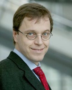
After an introduction into 3D laser nanoprinting and a brief review of the state-of-the-art in terms of spatial resolution and printing speed, I emphasize recent progress of my group, including rapid multi-focus multi-photon as well as multi-material multi-photon 3D laser nanoprinting. Furthermore, I shall cover our recent work on using two-step absorption instead of two-photon absorption which enables to replace expensive and large femtosecond lasers required in conventional setups by compact and inexpensive continuous-wave semiconductor laser diodes.
Biography
After completing his Diplom and PhD in physics at Johann Wolfgang Goethe-Universität Frankfurt (Germany) in 1986 and 1987, respectively, he spent two years as a postdoc at AT&T Bell Laboratories in Holmdel (U.S.A.). From 1990-1995 he was professor at Universität Dortmund (Germany), since 1995 he is professor at Institute of Applied Physics of Karlsruhe Institute of Technology (KIT). Since 2001 he has a joint appointment as department head at Institute of Nanotechnology of KIT, since 2016 he is one of its three directors. Since 2018 he is spokesperson of the Cluster of Excellence 3D Matter Made to Order.


